for IB = -10 µA, -20 µA, -30 µA, ... , -80 µA
big data file, smaller data file, postscript plot, pdf plot
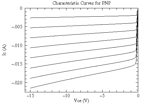
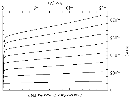
Note that you can make the PNP characteristic curves look like the
common NPN curves just by rotating the PNP plot by 180°. In swapping
N for P so NPN  PNP, we've reversed the direction of current flows
(so currents are negative -- flowing out of the collector and base in a PNP) and the
required supply voltage becomes negative for a PNP.
PNP, we've reversed the direction of current flows
(so currents are negative -- flowing out of the collector and base in a PNP) and the
required supply voltage becomes negative for a PNP.
That is to say that the PNP is designed for negative power supplies and out-flowing (negative) base and collector currents -- the opposite of NPNs.
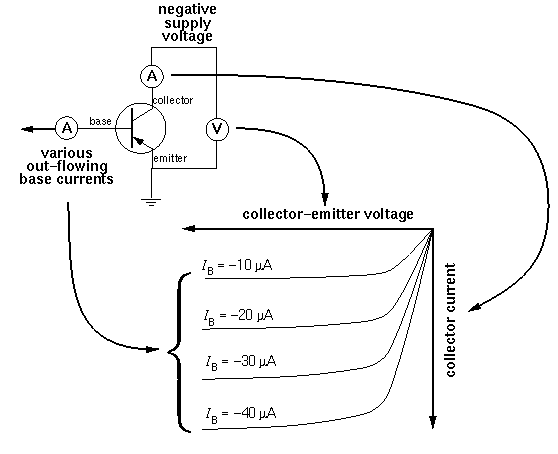
The behavior of a PNP bipolar transistor is largely controlled
by the current flowing out of the base.
For the usual collector-emitter voltage drops (i.e., the active region:
negative voltages from a fraction of a volt down to some breakdown voltage) the collector
current (IC) is nearly independent of the collector-emitter voltage
(VCE), and instead
depends on the base current (IB).
(This is unusual behavior: usually more voltage
produces to more current, but here the current only increases
slightly with increasingly negative VCE.) The current gain,
i.e., the ratio of the collector current to the base current, is
often denoted by  or hFE:
= hFE =
IC/IB
Thus in the simplest approximation the characteristic curves of a PNP are a set of flat, evenly spaced, lines:
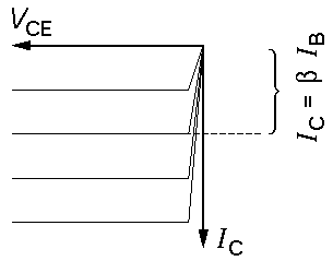
Each (flat) curve shows that IC doesn't change with changing VCE. The different levels show that IC does depend on IB.
A slightly more complicated approximation takes into account the sloping characteristic curves through a constant Early Voltage (VA). Here we assume that the characteristic curves all have a common x-axis intercept at the large positive voltage VA. (The dashed curves are far from the active region and in no way represent the actual behavior of the transistor for positive VCE. In fact, the PNP transistor is not designed to be operated with positive VCE.)
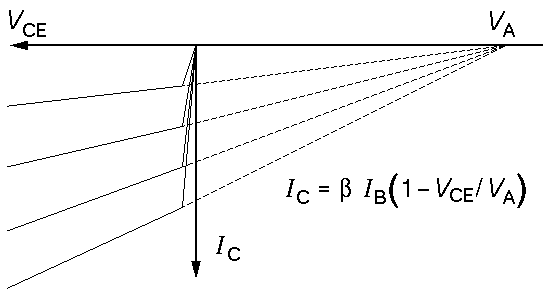
(For the above measured 2N3906, the Early voltage ranges from 40 to 50 V. That is the extrapolated characteristic curves do not intersect at a point.)
The actual relationship between the collector current (IC) and the controlling base current (IB) and collector-emitter voltage drop (VCE) is some complicated function which we can denote:
IC(IB,VCE)
Like any function we can approximate it near a particular point using just the first terms of a Taylors expansion:
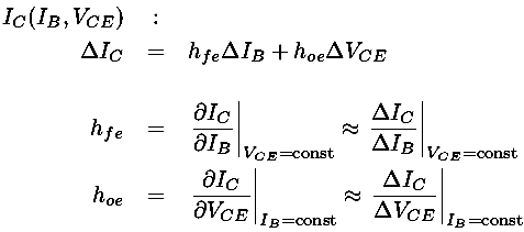
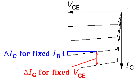
Clearly these hybrid (h) parameters are not constants.
For example hoe is the slope of a characteristic
curve, which is nearly zero for small |IB| and increases
for more negative IB. (Note that slope on an I-V
is basically the inverse of the resistance. Thus 1/hoe
can be described as the output impedance. A typical value for
1/hoe would be 100,000  .)
.)
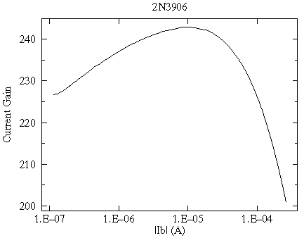
Even the defining parameter -- the current gain
or hFE -- is not exactly
constant and depends on IB. Here is the measured
relationship for the above 2N3906:
The characteristic curves focus on the output of the transistor, but we can also consider the behavior of the input. In the active region the base is a forward biased diode, and so VB would be about -.7 V, typical for a conducting Si diode. Of course in greater detail the relationship between VB and IB would be given by the Shockley diode equation:
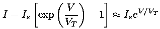
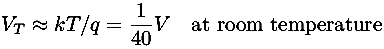
where Is is a constant and the thermal voltage VT is given by:
Because of the exponential relationship between base current and base voltage, the slope of this relationship (which could be called the input conductance, or 1/rB, or 1/hie) can be approximated by:
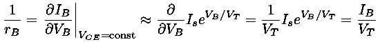
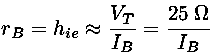
where in the last equation (25 /IB)
the absolute value of the base current must be entered in mA.
A desirable characteristic of a transistor is that the outputs have little effect on the inputs, but if we look in detail we find that VCE affects VB. The actual functional relationship giving the base voltage from the base current (IB) and collector-emitter voltage drop (VCE) is some complicated function which we can denote:
VB(IB,VCE)
Like any function we can again approximate it near a particular point using just the first terms of Taylors expansion:
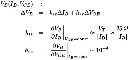
The small value of hre shows that the input is largely unaffected by the output.
The spec sheet reports the following values for the 2N3906:
| Characteristics | Symbol | Min | Max | Unit |
|---|---|---|---|---|
| Input Impedance | hie | 2 | 12 | k Ohms |
| Voltage Feedback Ratio | hre | 0.1 | 10 | ×10-4 |
| Small-Signal Current Gain | hfe | 100 | 400 | |
| Output Admittance | hoe | 3.0 | 60 | µ mhos |